![]() It is easy to combine Yoctopuce devices to build a complex system, like Lego bricks. But using micro-USB cables for interconnections is often not adequate to make a robust, compact and professional-grade solution. One possible alternative to USB cables is the use of small wires with 1.27mm connectors, much smaller, which can be soldered on all our devices. Today we are showing a second alternative, which also solves the question of fixing the complete system in a dedicated enclosure.
It is easy to combine Yoctopuce devices to build a complex system, like Lego bricks. But using micro-USB cables for interconnections is often not adequate to make a robust, compact and professional-grade solution. One possible alternative to USB cables is the use of small wires with 1.27mm connectors, much smaller, which can be soldered on all our devices. Today we are showing a second alternative, which also solves the question of fixing the complete system in a dedicated enclosure.
The solution is to create a custom PCB that will serve both as a fixing plate for holding the devices, and as electrical wire to connect them. You don't need to master electronics for designing such a simple PCB, and you don't even need to order more than two pieces to get it manufactured just for you. All you need is a proper PCB design software, and the component models for the Yoctopuce devices that you want to integrate. Guess what. this is what we are offering today.

Yoctopuce devices assembled using a custom PCB
PCB design software
There are multiple PCB design software of all kind. Between very limited novice products and highly expensive professional solutions, we have selected DipTrace for the following reasons:
- It has all important functions you need in a PCB design software.
- Il includes a 3D visualization feature to view what the final product will look like.
- Il includes a "one click" online PCB ordering system.
- The license is free for non-commercial use, and the price is very reasonable for professional use.
- It is available for Windows, Mac OS X et Linux.
DipTrace user interface
A PCB design software is only be a real help when it includes a component library corresponding to your project. This library has to include the dimensions of each component, as well as the exact position of their connection pads, to let you easily create PCB connections between components. DipTrace includes many standard components such as terminal blocks and connectors. We have just created a new add-on library for DipTrace, with the footprints for all Yoctopuce devices available until now. And we will continue to update this library in the future as new devices will be released.
We will now explain how to use DipTrace to create a PCB dedicated to assemble Yoctopuce devices.
NB: all steps described below are illustrated from A to Z in the video at the end of this article. If you prefer to see the steps being performed in front of you, rather than reading explanations, you can skip directly to the video.
Installing Yoctopuce Library for DipTrace
If not yet done, start by installing DipTrace, then download Yoctopuce library from our web site. The library is a simple zip file that you can extract in the directory of your choice, but that will have to stay at that place.
Start DipTrace, and select the "PCB Layout" tool. It is where the library must be installed.
- Open the Library menu, and select Library Setup.
- Click on User Components to add the Yoctopuce compoentn library in this group, and click on Add Library.
- Go to the place where you have extracted Yoctopuce library, and select the file with extension .emi
- Click on User Patterns to add Yoctopuce footprint library in this group, and click on Add Library.
- Go to the place where you have extracted Yoctopuce library, and select the file with extension .lib
- Clock OK to close this window
- Open the Tools menu, and under 3D Preview select Patterns and Models search....
- Click on Add to add the 3D models of Yoctopuce library
- Go to the place where you have extracted Yoctopuce library, and select the directory models3d
- Click OK to close this window.
That's it. Now if you click on the top of the component bar, on the left of the screen, you can choose the category User Components. You should be able to find there all Yoctopuce devices. You can then close the PCB Layout tool: the Yoctopuce library is installed properly.
Creating a custom PCB using DipTrace
To make a printed circuit board, you need to start by drawing its schema. So open the Schematic Capture Tool.
By clicking on the top of the component bar located left of the screen, choose the User Components category. This is where you will find Yoctopuce devices. Click on the device that you want to place, and move your mouse to the schema sheet. Before placing the component, you can turn it if needed using the space key. Click when you are happy with the position and orientation, and press ESC to switch to another Yoctopuce device.
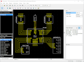
Once you have picked all the devices that you need, you must connect them. Use the Place wire tool to create logical connections between devices. To connect a device to a hub, you will need to connect the 4 wires. While drawing a wire, you can click on the sheet to place intermediate points to guide your wire. Don't worry if the connections don't look nice from the beginning, you will be able to arrange them afterwards. At this time, these are anyway just logical connections, not physical tracks, so their path is not so important. Wires in the schema can cross each other without problem.

Define logical connections between devices in the schema
Once your schema is done, save your work, then open the File menu, and select Convert to PCB. After an intermediate window that you can safely ignore for now, this will automatically start the PCB editor on a new document containing all devices that you have selected.

The selected devices are already present on the PCB, but you will have to organize them
This time, you see the actual shape of the Yoctopuce devices: their footprint. Clear blue lines show the connections that you have decided to make, according to the schema. You can now arrange the devices according to the desired position of the connectors, but also taking into account that you will want to keep the track connections (illustrated by the blue lines) as simple as possible.
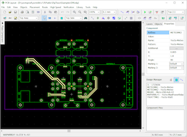
The next step is to perform routing, that is, drawing the electrical tracks that connect connection pads together. You can try to use the built-in auto-routing tool available in DipTrace if you want. We usually prefer to do the routing manually, because the auto-router tends to split groups of signals that we would prefer to keep together, such as power supply nets and USB bus. So we will use the Route manual tool. Click on one pad to connect, click on intermediate points where you want the track to go, until you reach the final pad indicated by the blue line. It is always safer to keep together all wires part of the same bus.
A simple PCB like this one has two layers: the top layer and the bottom layer. You can therefore choose to route some tracks on the top layer, and others on the bottom layer. To switch from one layer to the other, don't forget to change both combo menus in the toolbar. It is also possible to add vias within a track, to switch layer in the middle. But for such simple circuits, you will probably not need that.
Think twice before going with a track within the circle around fixing holes: depending on the layer, there could be a screw head ripping on the solder stop and causing a shortcut. Normally, you should expect screw heads to be on the bottom layer.

Draw the tracks that link together device connection pads
For connections that carry more current (like power supply), it is recommended to use larger tracks. To change the width of a track, you can right-click on it, select Net properties, enter the desired track with (e.g. 1mm) and select Apply to: Selected Net. You can also change the track width at the time you draw it, pressing the W shortcut key.
Once your circuit is fully routed, you can use the functions in menu Verification to check that there is no mistake. Don't forget to save your PCB from time to time.
At this point, you have not yet defined the position of the PCB borders. This can be done using the Place board outline tool. Usually you will want to select a larger grid while drawing the PCB borders, like 1mm for instance. Click on each desired PCB corner, then close the shape by double-clicking on the starting corner, and press ESC. You can move the corners afterwards if needed. Note that if you intend to mount your PCB in an enclosure, it might be a good idea to start by defining the PCB borders before placing the devices, in order to avoid a bad surprise at the end...
Once this last step is completed, you you can admire your work and run a last visual inspection: Open menu Tools, and select 3D Preview, 3D Visualization. DipTrace should confirm that Yoctopuce 3D models have been found, and then let you explore the system you have built under all angles. You can drag it while holding the left button to turn the assembly, roll the wheel to zoom, and drag it with the right button to move the assembly.

3D visualization gives a good impression of what the system will look like
If everything looks good, you can order the PCB. Using DipTrace, this is just a few clicks away: open the File menu, and select Order PCB. Vous will get an immediate price quote, which depends on the number of pieces ordered and the desired production turn time. Under 5 days, expect large price increases... Fill-in the form and click on Place Order. You will get a first mail to acknowledge your order, then once the shipping fees are known, a second e-mail with an invitation to pay the invoice through PayPal.
This is it, now you can wait until your PCB arrive with your mail. Don't be too impatient if you are outside US, customs will certainly add about a week to the production time...

The PCB arrived by registered mail
Assembly
To mount the devices on the PCB, you will need two accessories, available on Yoctopuce shop:
- fix-2-5mm, which contains 5 threaded spacers and 10 pieces of 2.5mm screw
- Board2Board-127, which contains 4 pairs of male/female board-to-board connectors, at a pitch of 1.27mm
You will most likely need one fix-2-5mm bag per device or hub to mount, plus half a bag of Board2Board-127 for each device to mount. Indeed, for each device, you will need one pair on the device side and one pair on the hub side..

Mounting devices on the PCB
Start by fixing the threaded spacers on the PCB. Then join the board-to-board connectors in male/female pairs, and insert them between the PCB and each device. The easiest way is usually to insert the pair first in the device, then to bring the device vertically close to the PCB. Fix the device to the spacers, and your board-to-board connector will be squeezed between the two, and will not move anymore.

Soldering the the 1.27mm board-to-board connectors
These connectors are quite easy to solder as they stay well in place. Use a good soldering iron with a fine tip, add flux to the contacts before soldering -this is a must- and if needed reread our tutorial that explains how to properly solder connectors. Make sure not to create bridges between contacts, and if you make one, remove it as described in the tutorial.
That's it, now you have your own product based on Yoctopuce devices, tailored as closely as possible to your needs, thanks to a custom PCB. All components are fixed with screw, all connectors are gold-plated, there is no hanging wire. This is the way to make it robust.
Tutorial video
For those that prefer a 10-minute video to a thousand words, here are the step-by-step instructions:

