_1.jpg) If you are interested in discovering how we create new USB modules, here is a peek at our prototyping tools. If you like it, we may go deeper on one topic or another in a future article.
If you are interested in discovering how we create new USB modules, here is a peek at our prototyping tools. If you like it, we may go deeper on one topic or another in a future article.
Everything starts with an idea for a new device. You may actually see some day in this blog (or in the "Vaporware" product category) such ideas when we decide to talk about them in advance. By the way, don't be shy, make your requests if there is a specific USB device that you would like us to create. We will add to our shop one new USB device per week if everything goes well...
Once we have the idea, we have to search for the electronic components specific to the product, e.g. the sensor. We mostly by them from Mouser, but for more exotic components or for smaller quantities, Farnell is good as well. Sometimes magic products are only available directly from the manufacturer, but that often means several weeks of delay.
All our components are organized in a database, at the core of our product design process, connected to every other design tool below. We put in it the specifications and datasheet of every component, including a very precise 3D model that we create ourselves. This may look like an overkill (and might actually be), but it really makes a difference for later stages of the process. We also create a footprint PCB model, directly from the manufacturer specifications.
Once the component is created in the database, it will automatically appear in our schema editor. We can then create an electronic schema for the new module, and transform it into a printed circuit board layout by routing each signal between components according to the schema. The routing tool shows what connection is missing, and constantly verifies that there is no violation of the routing rules set in advance. This way, the PCB designer can focus on optimally routing to minimize loops and crosstalk between signals while using as little space as possible.

Milled and tinned circuit board
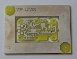
Here comes the prototyping. A first version of the circuit board is created by milling. Starting from a fiberglass copper plate, we automatically build a double-sided circuit board by removing the copper layer everywhere but on the signal tracks. The milling precision is enough to build prototype boards at the final 1:1 scale, even when using QFN chips. The resulting circuit board is then tin-plated to ease soldering by immercing the board into a solution of liquid tin for half a minute or so.
The prototype building steps will follow in part 2 of the article.


